


SI2302CDS-T1-GE3 N-Channel Power MOSFET
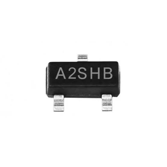
The SI2302CDS-T1-GE3 (base part number SI2302CDS, common SMD marking A2 with date/lot code) is a TrenchFET N-Channel Enhancement Mode Power MOSFET engineered for low-voltage, high-efficiency load switching and power management in compact portable electronics. Rated for a 20 V drain-source voltage and 2.9 A continuous drain current (10 A pulsed), it features ultra-low on-resistance down to 45 mΩ at Vgs = 4.5 V and 60 mΩ at Vgs = 2.5 V, enabling direct drive from 2.5 V, 3.3 V, and 5 V logic controllers. Housed in a miniature SOT-23 surface-mount package with 1.25 W total power dissipation, it is fully halogen-free and RoHS-compliant (-GE3 suffix) for battery-powered devices, DC-DC converters, and USB power switches.
Key Features:
- Ultra-Low On-Resistance: 45 mΩ (Max.) at Vgs = 4.5 V and 60 mΩ (Max.) at Vgs = 2.5 V minimizes conduction losses and voltage drop in low-voltage power paths.
- Sub-Logic-Level Gate Drive: Low gate threshold voltage (0.65 V Min. to 1.2 V Max.) guarantees full enhancement directly from 2.5 V, 3.3 V, and 5 V microcontroller GPIOs.
- High Current Density in SOT-23: Handles 2.9 A continuous drain current (10 A pulsed) and 1.25 W total power dissipation (t <= 5 s) in a compact surface-mount footprint.
- Fast TrenchFET Switching: Low total gate charge (3.9 nC Typ.) and fast switching times reduce switching losses in high-frequency DC-DC step-down and boost circuits.
Typical Applications:
- Load switching and power rail gating in portable, IoT, and battery-powered devices
- Low-voltage synchronous DC-DC converters and point-of-load (POL) regulators
- USB power distribution switches, Li-Ion battery protection, and charger control
- Low-side solenoid, relay, LED strip, and small DC motor drivers
Technical Specifications:
- Part Number: SI2302CDS-T1-GE3 (Base: SI2302CDS | SMD Marking: A2 | Halogen-Free & RoHS Compliant)
- Transistor Polarity: N-Channel Enhancement Mode MOSFET (TrenchFET)
- Mounting Type: Surface Mount (SMD)
- Package / Case: SOT-23 (SOT-23-3 / TO-236AB)
- Drain-Source Voltage (Vdss): 20 V
- Gate-Source Voltage (Vgss): ±8.0 V
- Continuous Drain Current (Id @ Ta = 25°C, t <= 5s): 2.9 A (2.5 A steady state)
- Continuous Drain Current (Id @ Ta = 70°C, t <= 5s): 2.3 A (2.0 A steady state)
- Pulsed Drain Current (Idm): 10 A
- Total Power Dissipation (Pd @ Ta = 25°C, t <= 5s): 1.25 W (0.96 W steady state)
- Drain-Source On-Resistance (Rds(on) @ Vgs = 4.5V, Id = 2.5A): 36 mΩ (Typ.), 45 mΩ (Max.)
- Drain-Source On-Resistance (Rds(on) @ Vgs = 2.5V, Id = 2.0A): 46 mΩ (Typ.), 60 mΩ (Max.)
- Gate-Source Threshold Voltage (Vgs(th) @ Vds = Vgs, Id = 250µA): 0.65 V (Min.) to 1.2 V (Max.)
- Forward Transconductance (gfs @ Vds = 10V, Id = 2.5A): 11 S (Typ.)
- Total Gate Charge (Qg @ Vds = 10V, Vgs = 4.5V, Id = 2.5A): 3.9 nC (Typ.), 6.0 nC (Max.)
- Input Capacitance (Ciss @ Vds = 10V, Vgs = 0V, f = 1MHz): 340 pF (Typ.)
- Output Capacitance (Coss @ Vds = 10V, Vgs = 0V, f = 1MHz): 115 pF (Typ.)
- Reverse Transfer Capacitance (Crss @ Vds = 10V, Vgs = 0V, f = 1MHz): 33 pF (Typ.)
- Operating Junction Temperature (Tj): -55°C to +150°C